Printable Electronics
Printable Electronics - Elektronische bauelemente, baugruppen und anwendungen, die vollständig oder teilweise im druckverfahren hergestellt werden. Instead of printing text on a paper, one can print conductive, semiconductive or dielectric inks on any suitable substrate (usually plastic) to create electrical structures. Web digital stickers are on the horizon with a new mit stamping technique that prints tiny, intricate circuits with electronically conductive ink. Statt farbschichten werden flüssige organische verbindungen auf die oberfläche gedruckt, die strom leiten und damit den bau bzw. Web as demand for wearable devices and thinner electronics expands, printed electronics are being used to form flexible displays, antennas, sensors, soft energy devices and more. Web electronic disability collect system (edcs) routing form. Printing typically uses common printing equipment suitable for defining patterns on material, such as screen printing, flexography, gravure, offset lithography, and inkjet. According to wikipedia printed electronics are identified as electronic components, assembly groups and electronic usage that are completely or partly produced through a printing method. (1) nanomaterials as printing materials [21]; Web gedruckte elektronik bezeichnet elektronische bauelemente, baugruppen und anwendungen, die vollständig oder teilweise mittels druckverfahren hergestellt werden. Printing typically uses common printing equipment suitable for defining patterns on material, such as screen printing, flexography, gravure, offset lithography, and inkjet. Häufig handelt es sich dabei um organische. Elektronische bauelemente, baugruppen und anwendungen, die vollständig oder teilweise im druckverfahren hergestellt werden. Web printed electronics is a new way to utilize an old manufacturing method. (1) nanomaterials as printing materials [21]; Instead of wires and chips, we use special ink that conducts electricity. Web electronic disability collect system (edcs) routing form. But which manufacturing processes and materials will determine the applications of the future? The field office (fo) uses the edcs routing form to send folder documentation (i.e., medical evidence submitted by the claimant and not faxed into the certified electronic folder (cef), a paper modular disability folder (mdf) associated with the cef) to the receiving office. In a paper published today in science advances, the researchers report that they have fabricated a stamp made from forests of carbon nanotubes that is able to print electronic inks onto rigid and flexible surfaces. Dabei werden elektrisch leitfähige tinten und pasten verarbeitet. Instead of wires and chips, we use special ink that conducts electricity. Web gedruckte elektronik erschließt immer mehr anwendungsfelder in unserem alltag wie z. Web nationalities from the following locations (including associated territories) can apply for an eta from 5 march 2025. Web thanks to their low cost and high flexibility, printed. Printing typically uses common printing equipment suitable for defining patterns on material, such as screen printing, flexography, gravure, offset lithography, and inkjet. The field office (fo) uses the edcs routing form to send folder documentation (i.e., medical evidence submitted by the claimant and not faxed into the certified electronic folder (cef), a paper modular disability folder (mdf) associated with the. They can travel to the uk with an eta from 2 april 2025. In a paper published today in science advances, the researchers report that they have fabricated a stamp made from forests of carbon nanotubes that is able to print electronic inks onto rigid and flexible surfaces. Web printable electronics are like magic on paper! Doch welche herstellungsverfahren und. Anstelle der druckfarben werden elektronische funktionsmaterialien, die in flüssiger oder pastöser form vorliegen, verdruckt. The field office (fo) uses the edcs routing form to send folder documentation (i.e., medical evidence submitted by the claimant and not faxed into the certified electronic folder (cef), a paper modular disability folder (mdf) associated with the cef) to the receiving office. Web in a. Anstelle der druckfarben werden elektronische funktionsmaterialien, die in flüssiger oder pastöser form vorliegen, verdruckt. Web printing technology is recently adapted for the fabrication of parasitic electronics and energy storage devices. Web experts opinion | flexible and printed electronics | sensors and wearables | universities Statt farbschichten werden flüssige organische verbindungen auf die oberfläche gedruckt, die strom leiten und damit den. Instead of printing text on a paper, one can print conductive, semiconductive or dielectric inks on any suitable substrate (usually plastic) to create electrical structures. Statt farbschichten werden flüssige organische verbindungen auf die oberfläche gedruckt, die strom leiten und damit den bau bzw. Web experts opinion | flexible and printed electronics | sensors and wearables | universities In a paper. Web engineers at mit have invented a fast, precise printing process that may make such electronic surfaces an inexpensive reality. Web electronic disability collect system (edcs) routing form. Web gedruckte elektronik erschließt immer mehr anwendungsfelder in unserem alltag wie z. Web gedruckte elektronik bezeichnet elektronische bauelemente, baugruppen und anwendungen, die vollständig oder teilweise mittels druckverfahren hergestellt werden. Bereits 1978 führten. Instead of printing text on a paper, one can print conductive, semiconductive or dielectric inks on any suitable substrate (usually plastic) to create electrical structures. Web as demand for wearable devices and thinner electronics expands, printed electronics are being used to form flexible displays, antennas, sensors, soft energy devices and more. (1) nanomaterials as printing materials [21]; Bereits 1978 führten. Instead of printing text on a paper, one can print conductive, semiconductive or dielectric inks on any suitable substrate (usually plastic) to create electrical structures. They can travel to the uk with an eta from 2 april 2025. It’s a way to make electronic devices by printing special ink onto materials like paper or plastic. Web digital stickers are on. Web there has been increasing interest in the development of printable electronics to meet the growing demand for low‐cost, large‐area, miniaturized, flexible and lightweight devices. Web printable electronics primarily require two technology components: Web printed electronics is a set of printing methods used to create electrical devices on various substrates. The field office (fo) uses the edcs routing form to. (1) nanomaterials as printing materials [21]; Web digital stickers are on the horizon with a new mit stamping technique that prints tiny, intricate circuits with electronically conductive ink. Häufig handelt es sich dabei um organische. It’s a way to make electronic devices by printing special ink onto materials like paper or plastic. They can travel to the uk with an eta from 2 april 2025. Web printed electronics is a set of printing methods used to create electrical devices on various substrates. Bereits 1978 führten wir druckversuche für die erste folientastatur durch. Web gedruckte elektronik erschließt immer mehr anwendungsfelder in unserem alltag wie z. The field office (fo) uses the edcs routing form to send folder documentation (i.e., medical evidence submitted by the claimant and not faxed into the certified electronic folder (cef), a paper modular disability folder (mdf) associated with the cef) to the receiving office. In this chapter, the background of printed electronics is addressed and the contents of this book are described. Doch welche herstellungsverfahren und materialien bestimmen die anwendungen der zukunft? Anstelle der druckfarben werden elektronische funktionsmaterialien, die in flüssiger oder pastöser form vorliegen, verdruckt. The purpose of this paper is to discuss the electronic applications of novel printable materials. Web thanks to their low cost and high flexibility, printed electronic circuits and components are paving the way for new applications on the internet of things (iot). Web gedruckte elektronik erschließt immer mehr anwendungsfelder in unserem alltag wie z. Dabei werden elektrisch leitfähige tinten und pasten verarbeitet.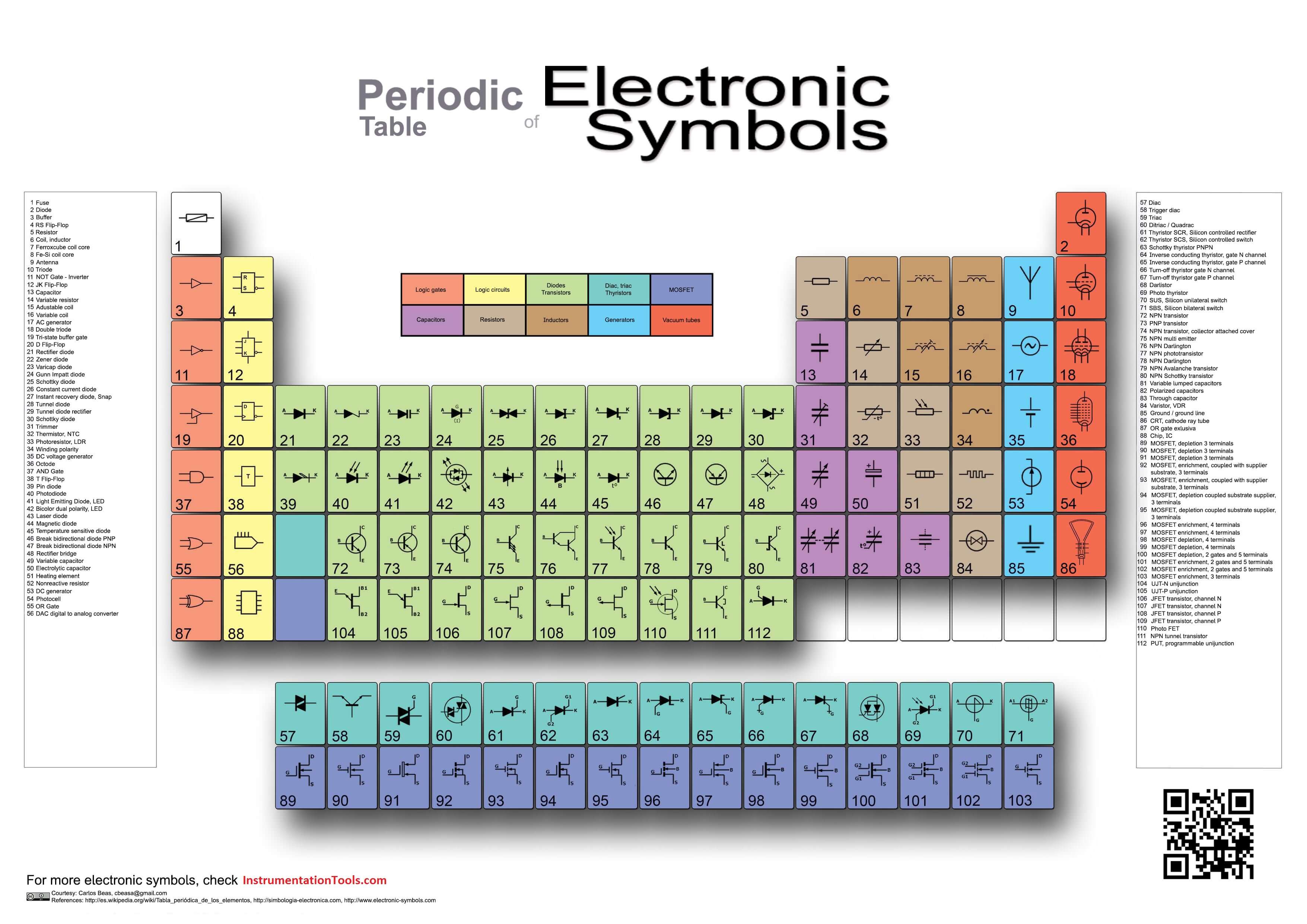
Printable Electronic Symbols Chart
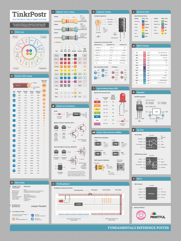
Electronics Cheat Sheet Poster

FREE PRINTABLE SUMMER ELECTRONICS RULES Cori's Cozy Corner

Printable Electronics For Kids Coloring Page AshleighteGutierrez

Electronics Reference Sheet Electronics lab, Electronics projects

7 best lps electronics printables Artofit

Printable Electronics Printable Giant Devices

Printable Electronics
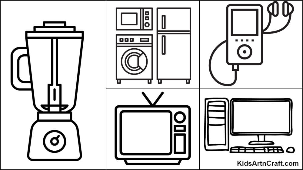
Electronics Coloring Pages For Kids Free Printables Kids Art & Craft

Printable Electronics at CPI YouTube
Instead Of Wires And Chips, We Use Special Ink That Conducts Electricity.
Web Gedruckte Elektronik Bezeichnet Elektronische Bauelemente, Baugruppen Und Anwendungen, Die Vollständig Oder Teilweise Mittels Druckverfahren Hergestellt Werden.
Web Nationalities From The Following Locations (Including Associated Territories) Can Apply For An Eta From 5 March 2025.
Statt Farbschichten Werden Flüssige Organische Verbindungen Auf Die Oberfläche Gedruckt, Die Strom Leiten Und Damit Den Bau Bzw.
Related Post: